TI-83 Teardown, Part 1
Starting off a teardown of some TI calculators to poke at their LCDs and see what happens.
Hey all!
Ordered a few dud TI calculators, a TI-83 Plus and two TI-86s, on Ebay a while back and finally have a use for them: their LCDs. I began to disassemble the TI-83 Plus to get to the LCD and took a few pictures of the process. Once I have the LCD, I've found another project that managed to get one working, but he's a lot more hardcore than I am so I'll be using an Arduino Mega to (hopefully) control it.
Part 1: Removing the LCD
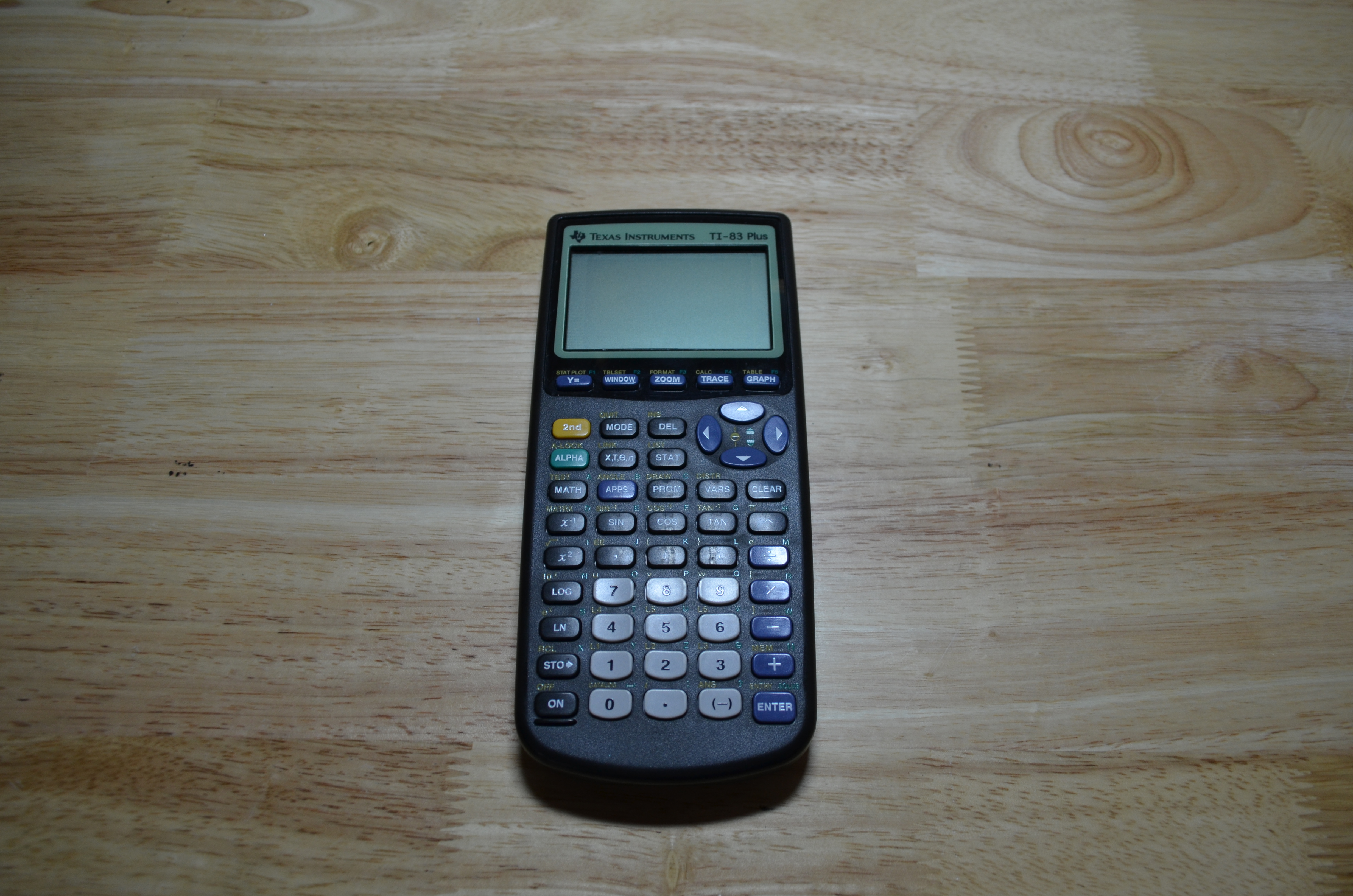
The front of the 83 looks nice, no scratches or anything. Too bad it'll never be functional again!
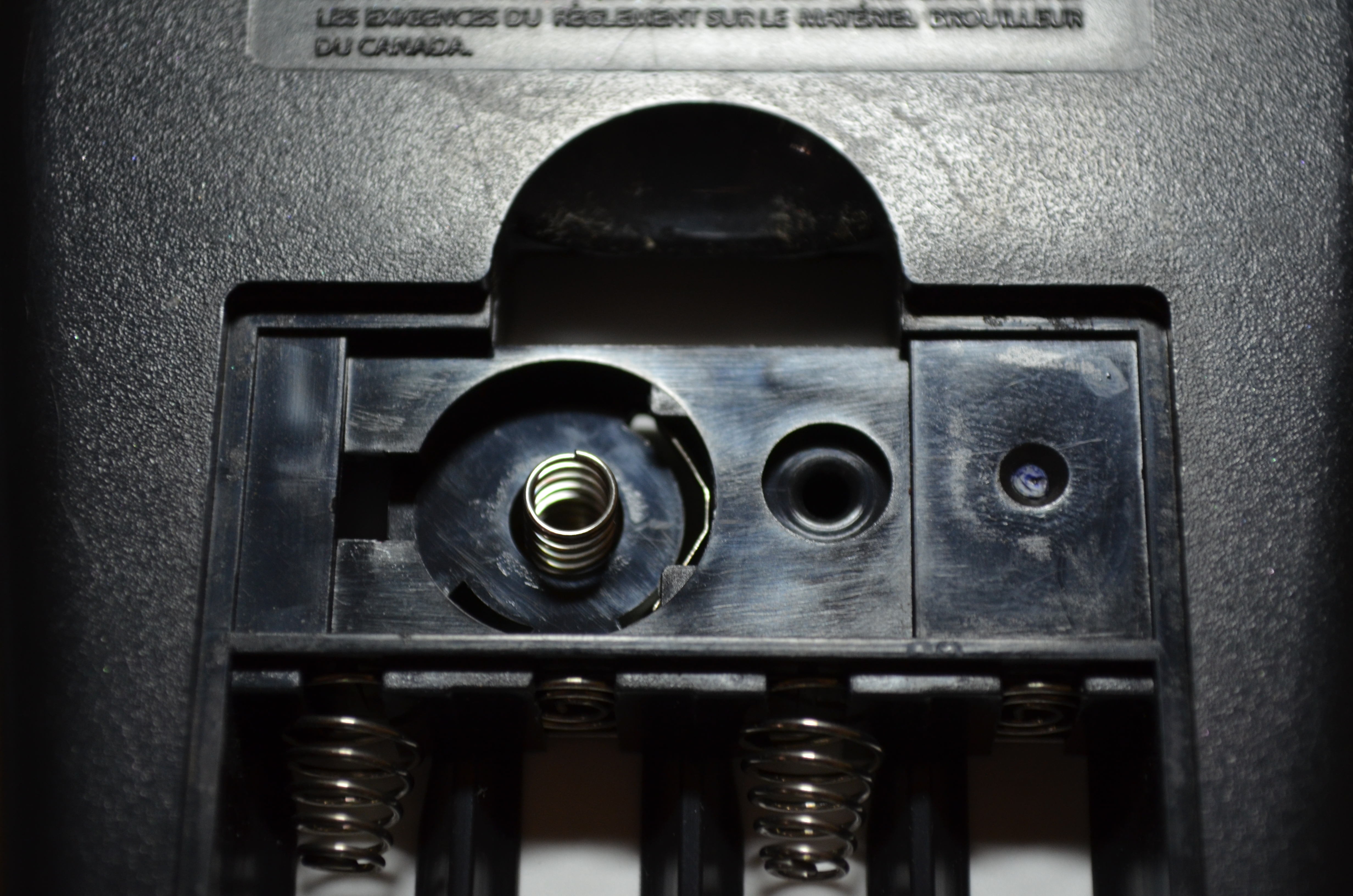
On the back of the 83 there were a few Torx-T6 screws that were fairly easy to get off, and a Phillips screw in the battery compartment (be sure to remove the backup battery!)
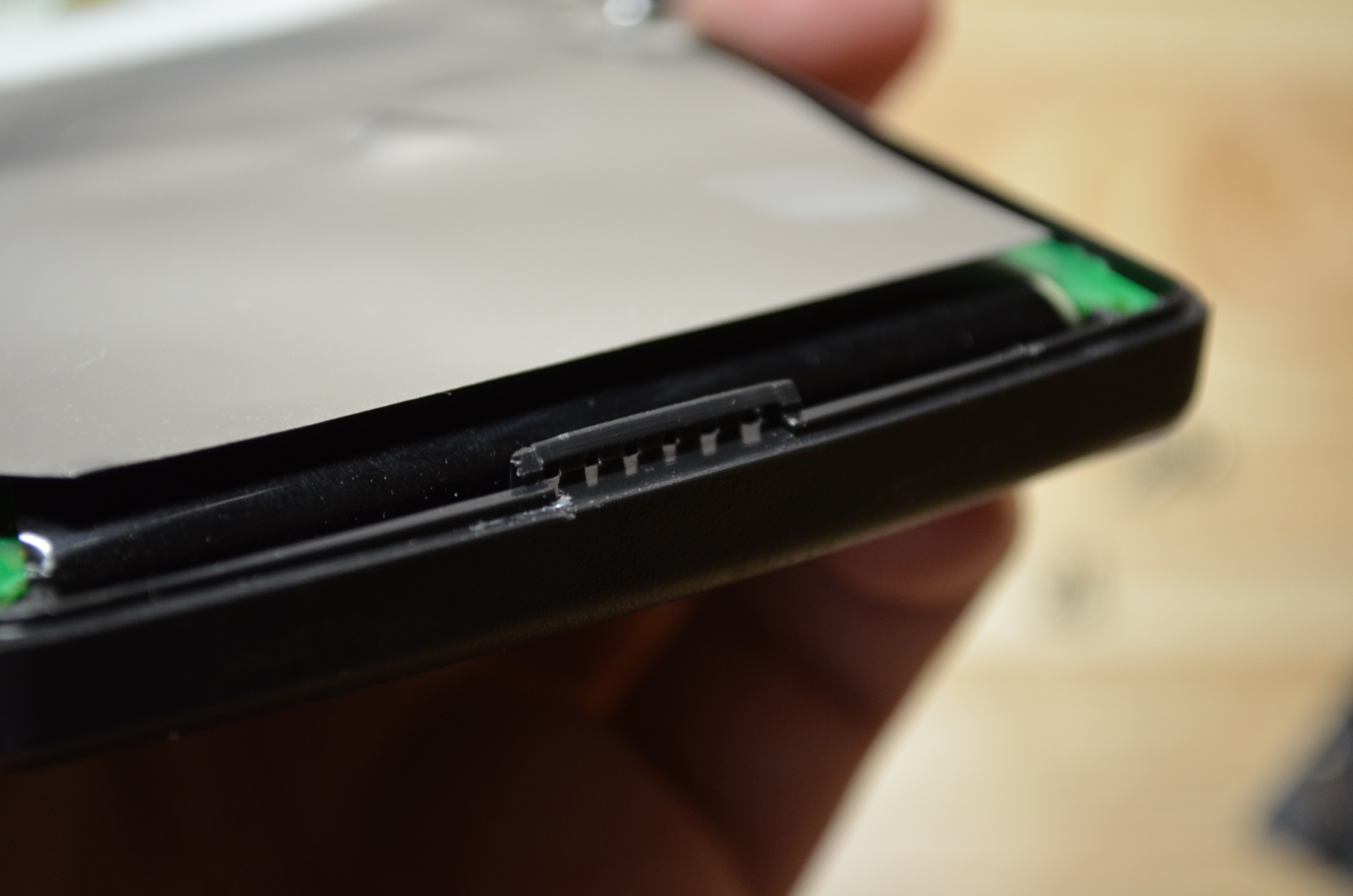
After that there was a series of clips, one on the top, above the screen, and two on the lower areas of the sides that need to be un-clipped (prying carefully with a thin, flat object seemed to do the trick). They look like this:
Once the case is off, you are presented with the interior! ...After you remove the board shielding. There're two Phillips screws down near the bottom. After that, there's a bit of adhesive under it that peels off fairly easy.
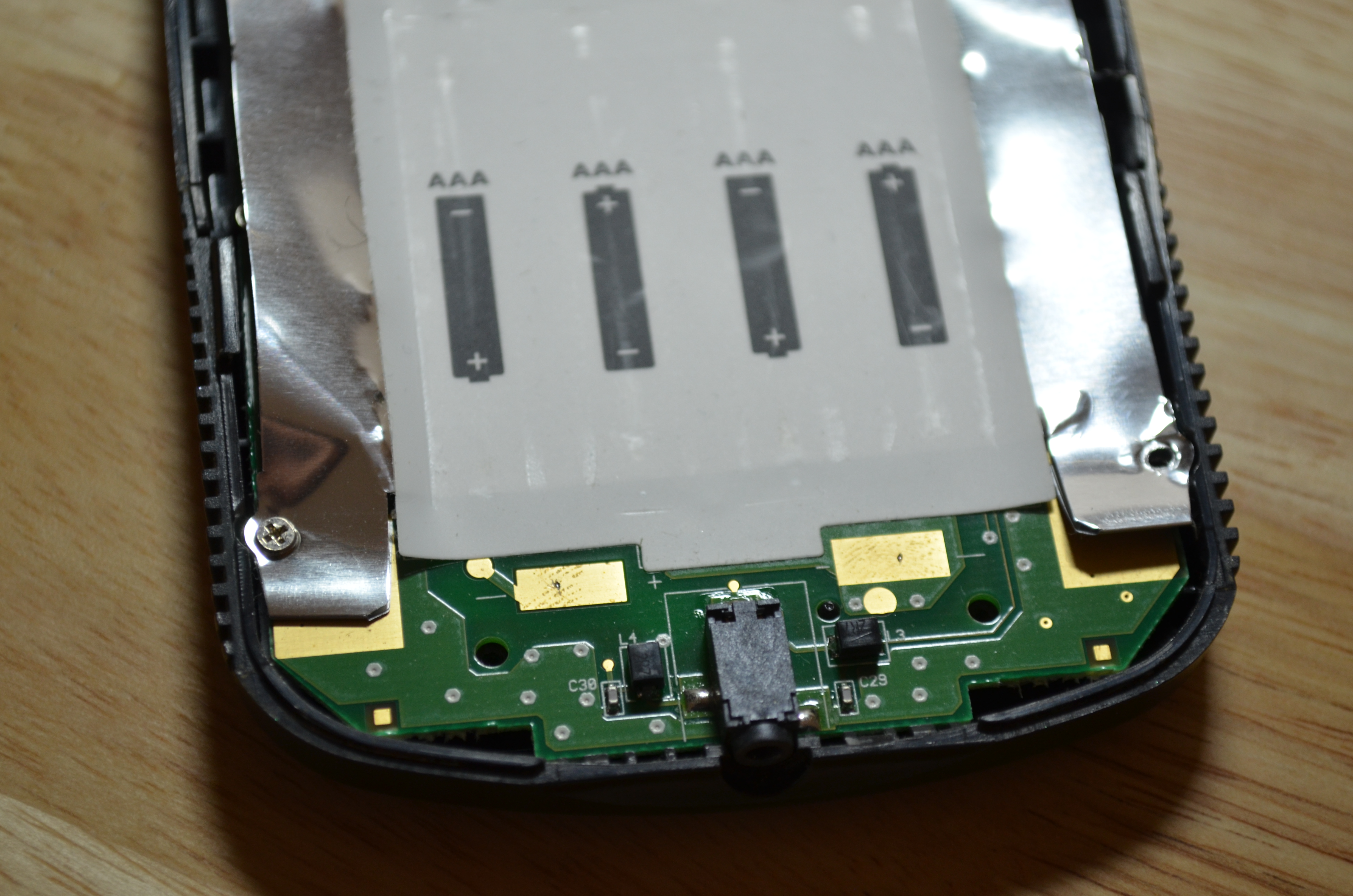
Once the shield's off, there are a few chips that stand out on the board at first glance:
- Inventec 6SI837, which, as far as I can tell, is an in-house 6MHz Z-80 processor
- Fujitsu MBM29LV400TC 512KB Flash memory
- 2x Fairchild MBM29LV400TC voltage interface transceivers
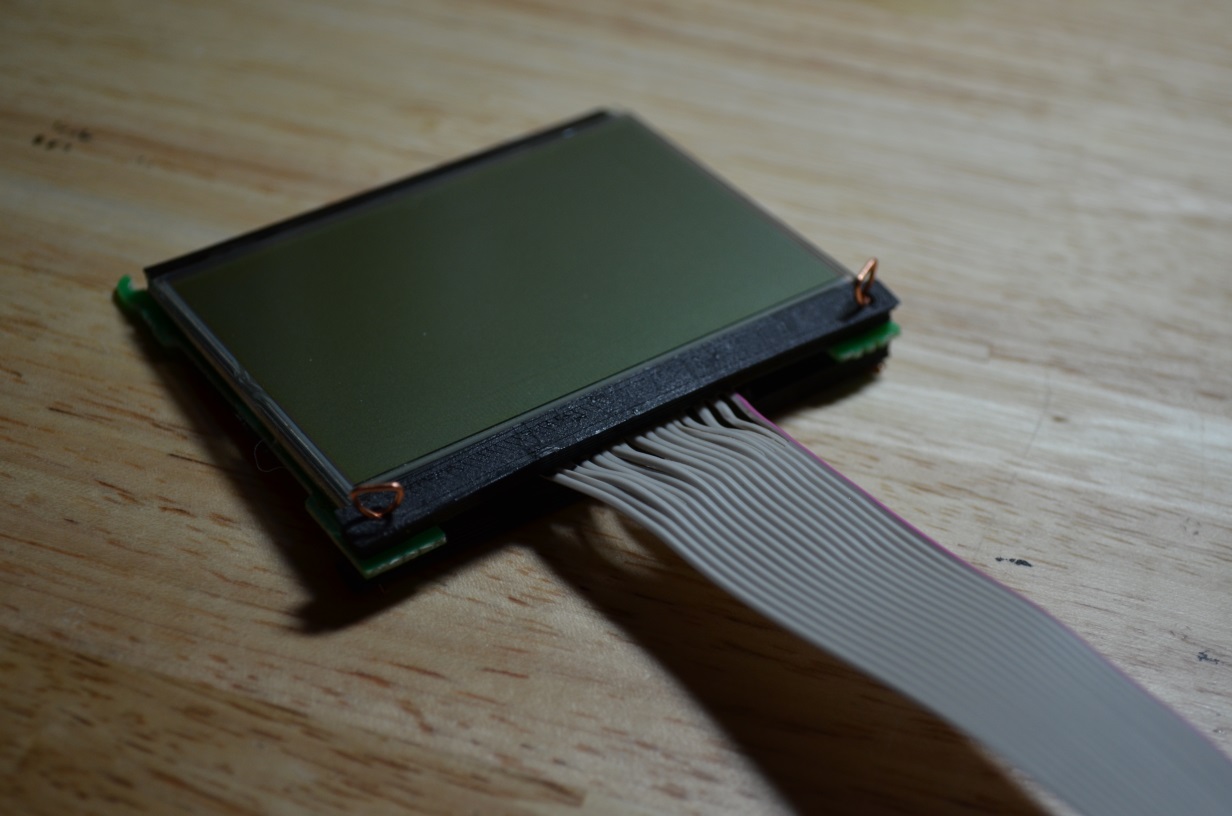
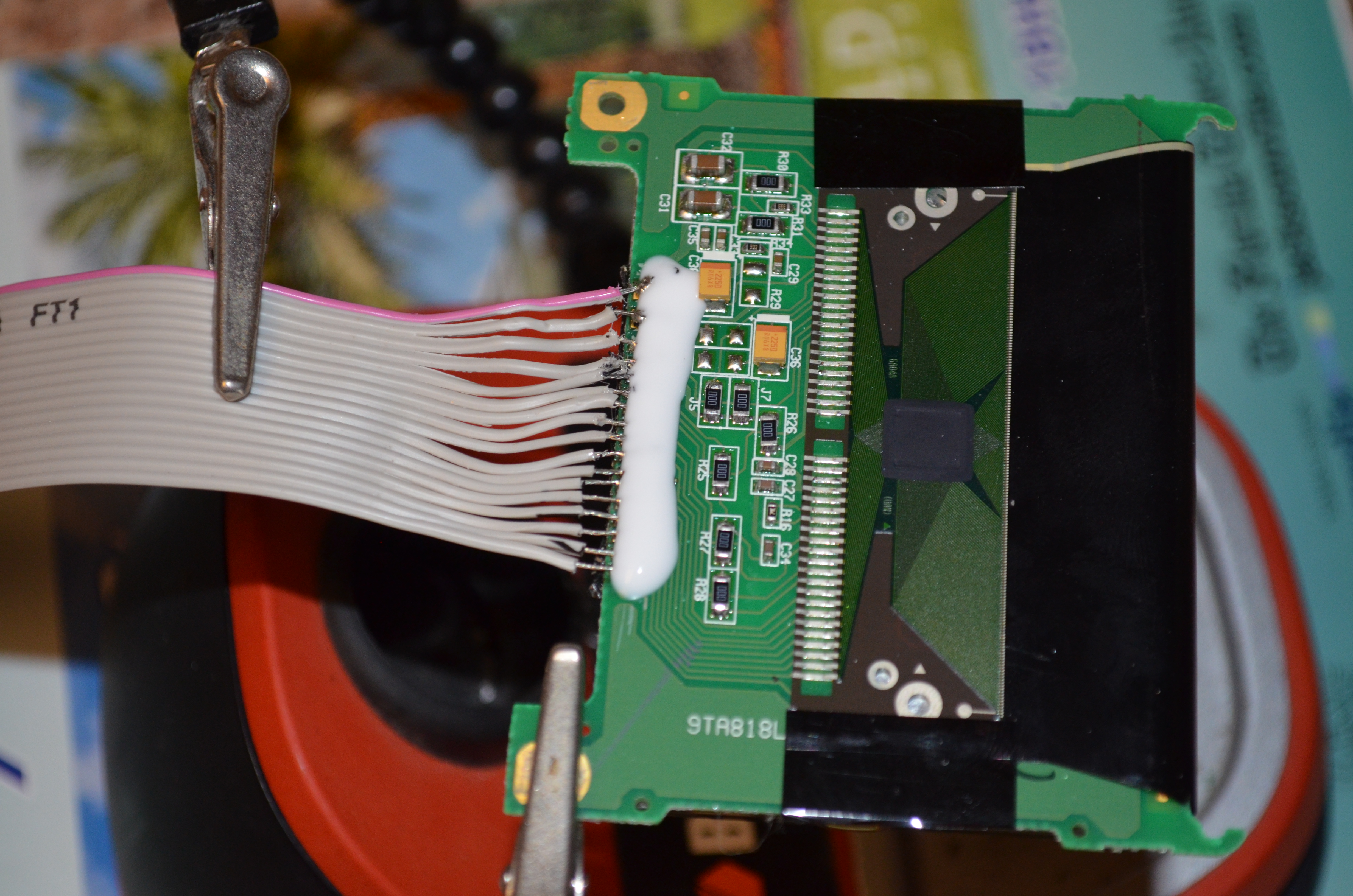
At the top, the display is mounted onto a daughter board, which is controlled by the main board via a ribbon cable. On the bottom sides, there are 2 more Phillips screws which hold down the daughter board. I removed these and, being unable to mount the irregular ribbon cable to an Adafruit Multi-pitch FPC Adapter, removed the cable entirely and carefully scratched the adhesive off the copper pads on the daughter board. I found an old IDE connector cable and cut it down to be a 2x9 connector (the one on the left) to fit the board's 17 pins.
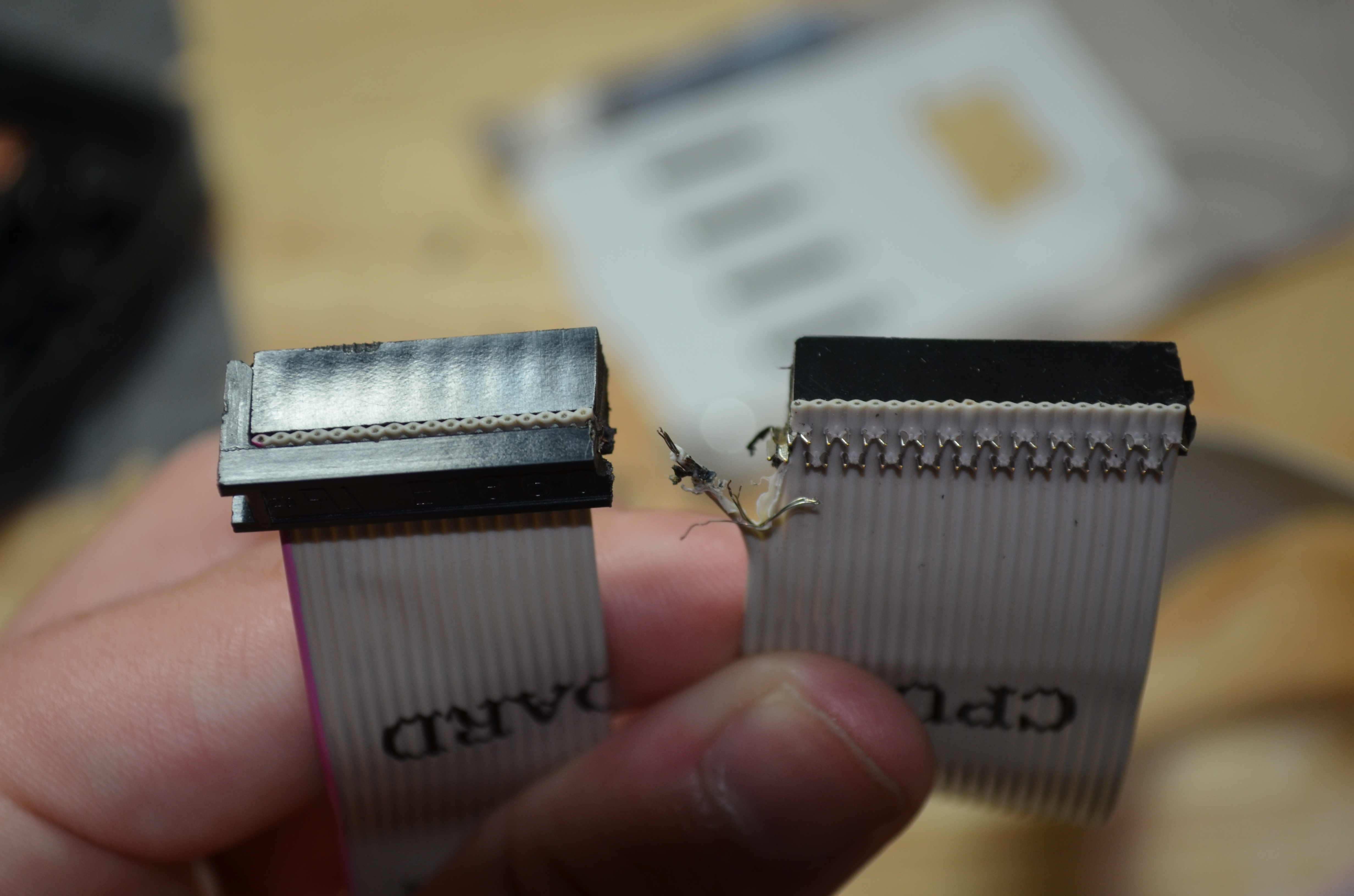
I spliced the cable and stripped the ends to prepare for the solder nightmare:
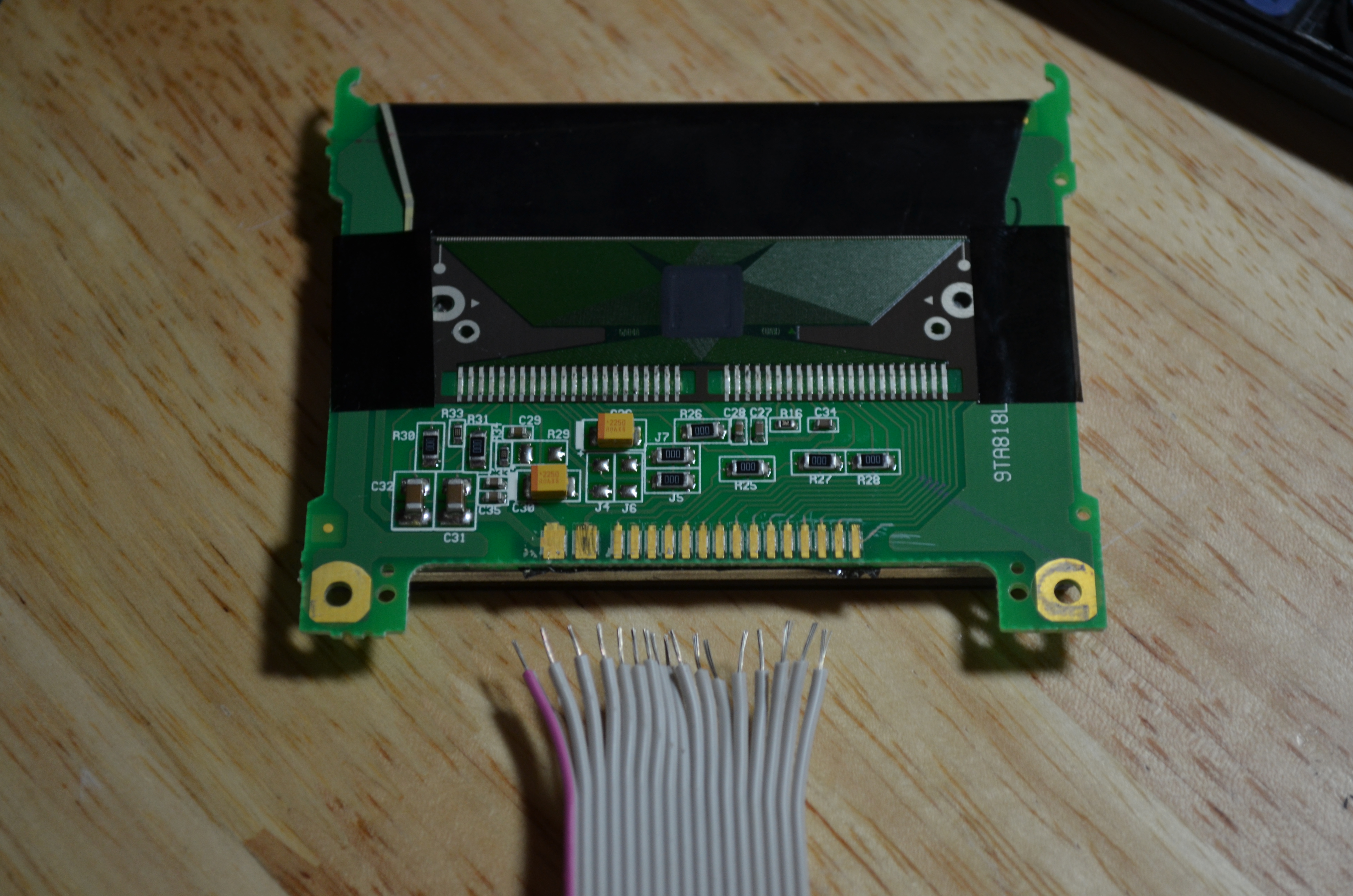
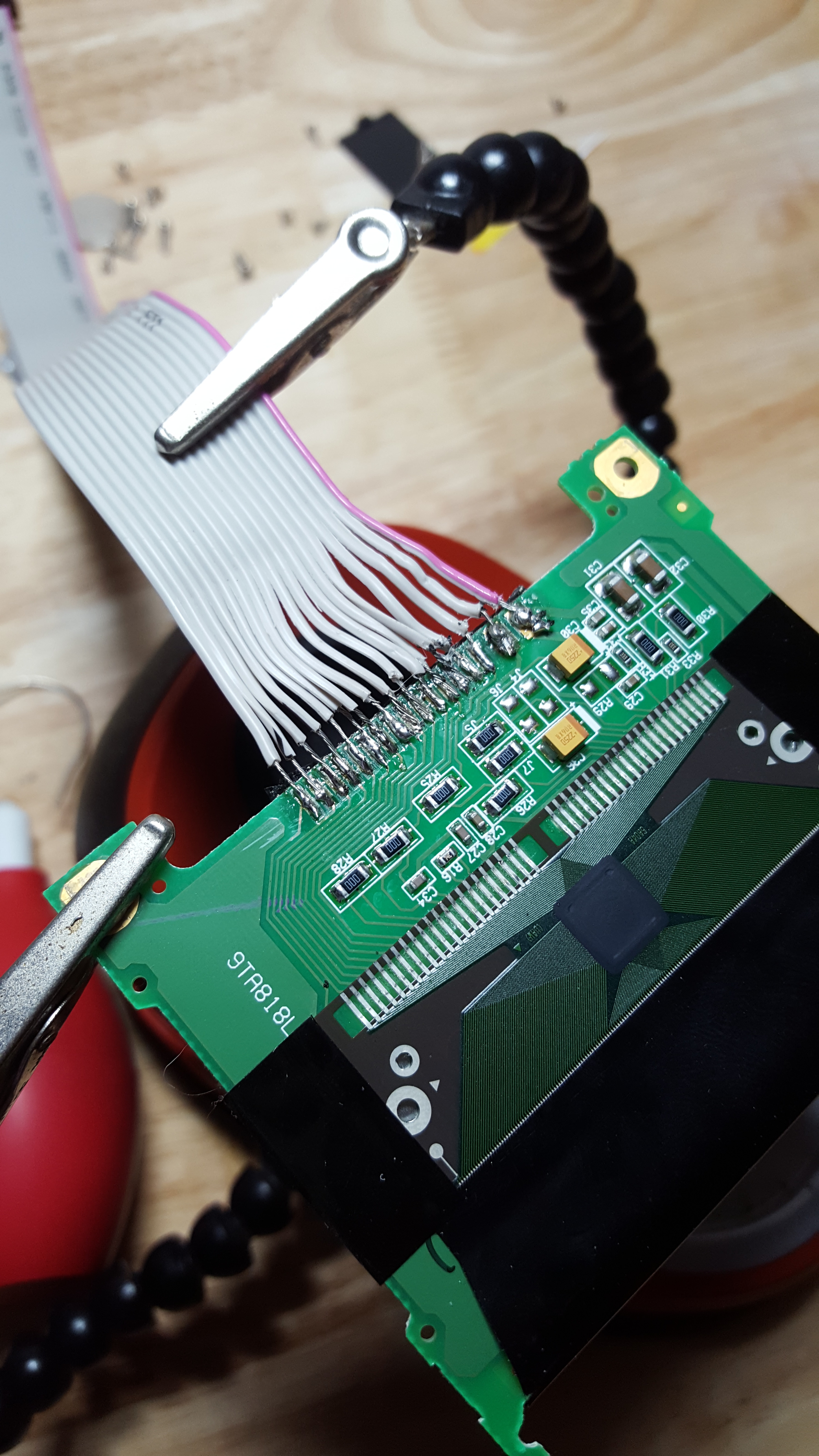
The solder job took about a half-hour and I coated the connections in glue (Elmers, didn't have epoxy on-hand, unfortunately) to try and decrease the chance i'll rip them off when I move the cable.
Next comes the fun part: programming!